


NEDO and Toshiba Develops World’s Largest Film-based Perovskite Photovoltaic Module
―703 cm2 module achieves 11.7% power conversion efficiency―
June 18, 2018
New Energy and Industrial Technology Development Organization (NEDO)
Toshiba Corporation
New Energy and Industrial Technology Development Organization (NEDO) and Toshiba Corporation (TOKYO: 6502) have developed the world’s largest film-based perovskite photovoltaic module. The module is 703 cm2 and realizes a power conversion efficiency (PCE) of 11.7%, overcoming the difficulties of increasing size and efficiency at the same time. The module was realized with meniscus printing technology owned by Toshiba and a newly developed printing process. Alongside its size and efficiency, the flexibility and lightness of the module is expected to open up possibilities for use in a wide range of locations.
NEDO and Toshiba will continue work to enlarge the module and to boost its efficiency to that of crystal silicon photovoltaic modules by improving the printing technology and materials used in the perovskite layer. A part of the encapsulation technology used in the module was developed in cooperation with Sekisui Chemical Co., Ltd. The ultimate goal is to achieve photovoltaic modules with a levelized cost of electricity of 7 yen per kWh by 2030.
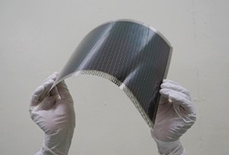
24.15 x 29.10 cm, 703 cm2
1.Overview
Crystalline silicon photovoltaic modules are the most widely used photovoltaic modules, but their weight and form factor limit possible installation locations. Film-based perovskite photovoltaic modules*1 are flexible and light, making possible various uses, including installation on buildings with load bearing weights too low for silicon cells, and installation on walls—advantages that could support the development of net zero energy building and net zero energy house (ZEB and ZEH). Moreover, since they are made with inexpensive materials and can be formed by printing, perovskite photovoltaic modules can be manufactured at low cost. For all these reasons, they are attracting attention as the next generation of photovoltaic modules.
However, while a small 0.09 cm2 perovskite cell realizes a PCE of 22.7%*2, close to that of crystal silicon photovoltaic modules, PCE decreases significantly with size, due to technical difficulties in forming uniform layers on the film substrate; until now, film-based modules larger than 15 x 15 cm2 have not been realized.
Toshiba has overcome these obstacles and developed a 24.15 cm x 29.10 cm film-based perovskite photovoltaic module, the world’s largest, with an area of 703 cm2 and PCE of 11.7%*3. The project was funded by NEDO*4 and uses Toshiba’s meniscus printing technology*5 and a new printing process.
Productivity improvements and weight reductions are expected to realize installation of perovskite photovoltaic modules at sites where standard photovoltaic modules cannot be used. Toshiba will continue to develop printing technology to enlarge the size of module and aims to expand the size to 900 cm2, the scale needed for practical application. It also aims to increase the PCE to a level comparable to that of crystalline silicon photovoltaic modules by improving the materials in the perovskite layers. The goal is to realize photovoltaic modules with a levelized cost of electricity of 7 yen per kWh by 2030.
The new prototype module will be displayed at the NEDO booth at the 13th Grand Renewable Energy International Exhibition, at Pacifico Yokohama from June 20-22, 2018.
2.Achievements
Toshiba developed the printing process for a larger module by controlling the chemical reaction between PbI2 and MAI on the substrate, using the ink composition as a mechanism. The company has also improved the uniformity of the layer thickness and increased the homogeneity of the crystal layer properties over a larger area, by controlling the process and adjusting the perovskite crystal growth conditions during the printing process. As a result, a PCE of 11.7% has been obtained on a module with an area of 703 cm2, almost as large as 900 cm2, the practical a scale. It is a step closer to practical application.
-
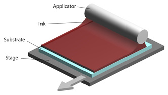 Figure 2. Applicator Ink Substrate Substrate stage
-
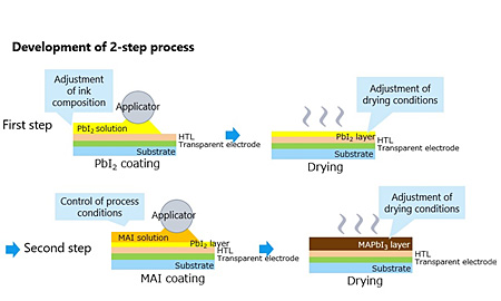 Figure 3. Development of 2-step process
Glossary
- *1: Photovoltaic modules where the active layer is made up of perovskite crystals
- *2: The highest PCE of small sized perovskite photovoltaic modules. Source: Korea Research Institute of Chemical Technology (KRICT).
- *3: PCE measured by the National Institute of Advanced Industrial Science and Technology, an internationally certified measurement institution. The maximum power point tracking (MPPT) method, the best measurement of PCE during actual usage, was used for the measurement. (The PCE by I–V measurement method was 11.5% for the forward sweep and 11.4% for the reverse sweep.)
- *4: Development of high performance and reliable PV modules to reduce levelized cost of energy / Research and development of innovative new structure solar cells / Development of perovskite-type innovative solar cells with low production cost (Development of super lightweight PV module technology)
- *5: Printing technology that uses the interfacial tension of the liquid material.
3.For more information, please contact:
NEDO New Energy Technology Department
Contact Person: T.Sato, T.Kunikawa
Tel: +81-44-520-5277
Toshiba Corporation
Public Relations & Investor Relations Div.
Tel: +81-3-3457-2100, E-mail: media.relations@toshiba.co.jp
Corporate Resarch&Development center
Tel: +81-44-549-2056, E-mail: inquiry@rdc.toshiba.co.jp