Development of Technologies for Super Energy-Efficient Optical Electronics Implementation Systems
Project overview
PL: ARAKAWA Yasuhiko (Professor, University of Tokyo)
Due to the development of cloud computing, the amount of processed information and communications traffic at data centers, is exponentially increasing, and, as a result, the amount of power consumption related to these activities is expected to rapidly increase. Therefore, there is a desire to achieve technology that makes possible information technology equipment offering both higher speeds and lower power consumption.
Today's information technology equipment and other electronics use electrical signals to transmit information between LSI chips* or circuit boards in order to process information. Information transmission speeds are being increased to accelerate information processing speeds for such equipment. However, the electrical wiring used to transmit electrical signals possesses electrical resistance, and the amount of heat generated by wiring increases in proportion to the transmission speed of the electrical signal. Therefore, increased transmission speeds of electrical signals naturally result in increased power consumption.
The goal of this project is to employ optical signal communications that make information transmission possible at higher speeds and with lower levels of power consumption than electrical signal communications used to transmit information between LSI chips in information technology equipment. The aim of this activity is to achieve technology that makes possible higher transmission speeds, lower energy consumption, and miniaturized information technology equipment. Therefore, this project involves the development of the following: electric-optic conversion technology to change electrical signals input/output by LSI chips to optical signals; optical wiring technology to transmit optical signals at high speeds; transmission and other underlying technologies; and technologies necessary to integrate the above technologies. The aim is to establish basic technology for achieving photonics-electronics convergence system technology fused with electronic circuit technology.
*LSI chips: large-scale integrated circuits
-
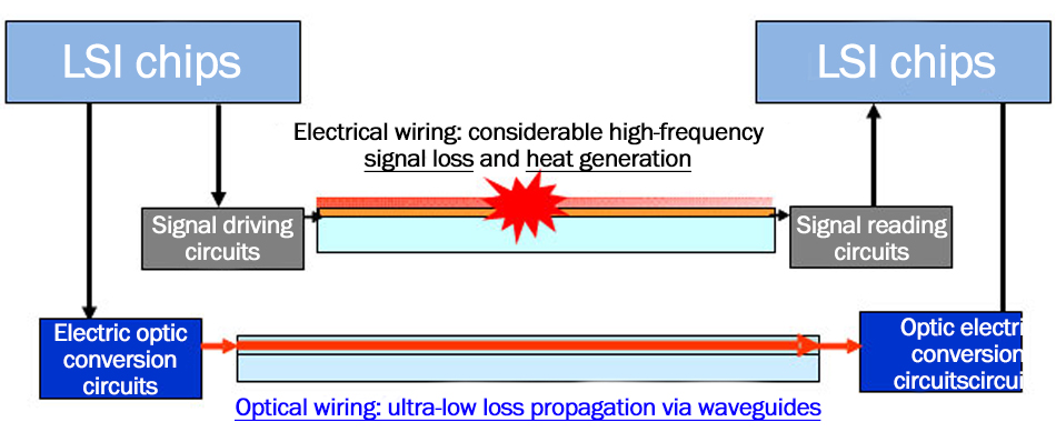 ■ Optical wiring characteristics
 -
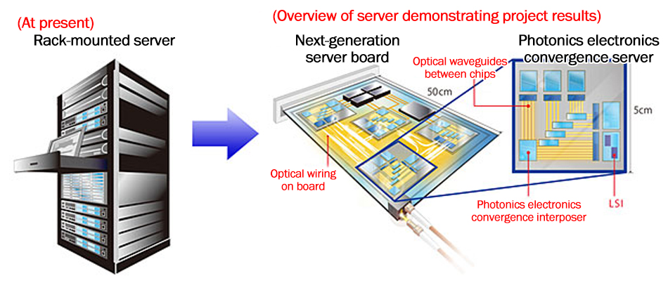 ■ Photonics-electronics convergence system (photonics electronics convergence server)
Basic information
| Technical field |
|
Project code | P13004 |
|---|---|---|---|
| Department in charge |
|
||
Last Updated : April 26, 2022